
As there is no direct coupling from the input to the output, terminating the Miller effect and providing a greater bandwidth. This combination contains several characteristics as compared to the single amplifier stage. Some of the characteristics are; greater output–input separation, greater input impedance, greater input impedance, and greater bandwidth also.

Figure 1 Combination of common-base & common emitter
The Cascode Configuration:
A prime amplifier configuration is called a “Cascode Amplifier”. It contains a CE i.e. common emitter stage subsequently a CB i.e. a common base stage. The CE i.e. Common Emitter configuration provides a comparatively greater input resistance ac e (β + 1) * r to the source at the signal.
A minimum input resistance i.e. er is provided by the Common base configuration. In the common emitter i.e. CE amplifier stage connecting the collector resistance that is RC to the CB i.e. Common base amplifier stage, the Miller effect of Cu1 is surely deducted by the CECB configuration. Through this, 3db or higher frequency can be achieved that can be achieved only with the help of a Common emitter amplifier. The collector of Q2 contains an exact current equal to the Q1 collector current, so an increase in the upper cut-off frequency is obtained regardless of minimizing the mid-band gain that is from the Gain bandwidth rule. Another purpose for increasing the above cut-off frequency is for the case of Common Base configuration the Miller Effect does not exist and also doesn’t bind the response by high frequency. The observation about the effective load resistance noticed by the Common Emitter transistor i.e. Q1 is very minimum and almost equivalent to input resistance that is er of the Q2 that is Common Base Transistor. The Q2 transistor behaves as a current buffer and also as an impedance transformer.

Figure 2 Configuration of cascode amplifier
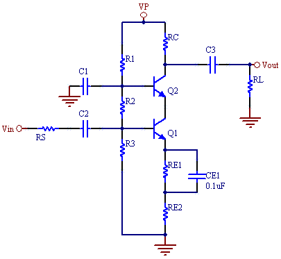
Components of the Cascode Amplifier
The following amplifier is a dual-stage amplifier, containing a Common Emitter stage that comes after a CB stage i.e. Common Base stage. This arrangement also provides notable advantages, such as bandwidth, gain, and stability. Let’s move towards the details of components and their roles.
I. Q1 (Common Emitter Stage)
Base: The Input Signal Application
At Q1, the base is applied to the input signal. The key process of amplification begins here. The current is controlled by the signal at the base with the help of a transistor, which is significant for the amplification process.
Emitter: Stabilization with a Resistor (RE)
The resistor RE is grounded and is connected to the emitter Q1. This setting helps the stabilization of Q1 which is the operating point of it. Negative feedback is provided by the resistor RE, which braces the operating point of the transistor that is against the changes in the parameters of the transistor and temperature. This stability is necessary for sustaining the compatible characteristics of amplification.
Collector: Connection to Q2’s Emitter
The emitter of Q2 is connected to the collector of Q1, producing the cascaded structure which explains a cascade amplifier. This connection certifies the current that is amplified from Q1 directly affects the operation of Q2, beneficially sending the signal from one stage to the other without any reasonable distortion or loss.
II. Q1 (Common Base Stage)
Base: Biasing with a Stable DC Voltage (V_B2)
A strong DC Voltage (V_B2) is biased with the base of Q2. A Voltage driver network is used for biasing. It consists of two resistors connected in a series connection between the ground and the power supply. The essential stable bias voltage at the base of q2 is provided by the center point of this network. The complete biasing is vital as it makes the operating point of Q2, securing it works in the right region for the amplification.
Emitter: Connection from Q1’s Collector
The collector of Q1 is connected to the emitter of Q2. This setting acknowledges the amplified signal by Q1 to send it directly to Q2. The maximum input resistance and minimum output impedance are provided by the common base configuration of Q2 that converts it to a successful point for additional amplification of the signal obtained from Q1.
Collector: Connection to the Power Supply (V_CC) through a Load Resistor (RC)
The power supply (V_CC) is connected to the collector with the help of a load resistor (RC). With the help of Q2, varying current is converted by the resistors which can be used as output signal. An important part is being played by the RC value for examining the output impedance and overall gain of the amplifier.
Bandwidth Capacitance and the Miller Effect
The Miller effect is the way to understand the wide bandwidth of the Cascode configuration. This effect is the product of Voltage gain Av by the bandwidth collector-base capacitance. The E-B (Emitter Base) capacitance is greater than the C-B (Collector Base) capacitance. Thus it can be concluded that C-B (Collector Base) capacitance would create a minimal effect. Also, in the C-E configuration the input at the base is out of phase with the collector output signal. The base signals are repelled by the collector signals capacitively paired. Moreover, the base signals are (1-Av) times less than the collector feedback. Take into account that for the inverting C-E amplifier, Av is a negative number. So the little C-B (Collector Base) capacitance appears (1+|Av|) times greater than its original value. The frequency increases with the capacitive gain reducing feedback and reducing the higher frequency response of a C-E amplifier.
-RL/ rEE is the approximate voltage gain of the Collector-Emitter (C-E) amplifier.
By biasing, the emitter current is adjusted to 1.0 Ma
REE = 26 mV/ IE = 26 mV/1.0mA = 26 Ω
So, Av = -RL/REE = -4700/26 = -181
A common base configuration is not linked with the Miller effect as the grounded base supports the collector signal from being transferred to the emitter input. However, a C-B (Collector Base) amplifier contains the highest frequency response comparatively. To contain little high input impedance, the CE level is enticing. The way is to lessen the gain (i.e. 1) of the Miller effect which is being reduced by the C-E stage i.e. C-B feedback to 1*CCBO. The total C-B (Collector Base) feedback is 2*CCBO that is the feedback capacitance is 1*CCB + the actual CCB capacitance. This is a significant subtraction from 181*CCBO. The miller for the gain of the -2 Collector Emitter (CE) stage is Cmiller = Ccbo(1-Av) = Cmiller = Ccbo(1-(-1)) = Ccbo*2.
The method to minimize the CE Collector Emitter gain is the load resistance to be reduced. RC/ RE is the gain of the CE amplifier approximately. The resistance is 26Ω for the internal emitter resistance Ree at the value of 1mA emitter current. For the explanation of 26Ω, look at the “Derivation of REE”. The resistance of the emitter of the C-B (Collector Base) stage loading the CE (Collector Emitter) stage is the collector load RC, 26Ω again. The CE (Collector Emitter) gain amplifier is around Av = RC/ RE = 26/26 = 1. The Miller capacitance is Cmiller = Ccbo (1-Av) = 8pF (1-(-1) = 16pF. At this point, we get a bit high input impedance CE stage without any distraction towards the Miller effect with no Collector Emitter (CE) Voltage gain db. A large number of voltage gain is received at the point of the CB stage i.e. Av = -181. β of the CE stage is the current gain of the cascade, and CB is 1 β completely. So, the cascade has a minimal greater input impedance of the CE, overall good gain, and a good bandwidth of the CB.

Figure 3 Cascode & common emitter CE for the comparison
Advantage and Disadvantages
This type of amplifier configuration contains a common base stage and a common emitter stage. Therefore, there is no direct coupling of output to the input but the cascade betters the input-output separation that reduces the reverse transmission. The outcome is, that the Miller effect is excluded and in return, the bandwidth is much larger.
The vacuum cubes and transistors are being used for the amplifier designs in which the Miller effect occurs. During an amplification process, we see how a comparatively little input impedance presents itself as much greater than the input of an amplifier. The process results in undesirable frequency response instability in the amplifiers.
As they can provide good bandwidth and gain, cascade configurations are utilized in Radiofrequency (RF) and other higher-frequency applications. The single transistor amplifiers are less complicated as compared to cascade configurations. So critical biasing should be checked to make the proper insulation.
The cascade amplifier configuration has various advantages and disadvantages:
Advantages
· This type of configuration is recognized because of its various advantages in the field of electronic circuit design, basically because of its capacity to reduce the Miller effect, get broad bandwidth, and also provide larger voltage gain. A common feature of this configuration is its ability to lessen the Miller capacitance effect, that exactly increases the overall performance and stable system.
· In a conventional amplifier system, this effect can be a cause for the increase in effective input capacitance, which can limit the speed and the bandwidth of the amplifier. This effect stands from the response capacity between the output and the input that is being amplified by the gain of the circuit. Moreover, in a cascade configuration, a Miller Capacitance effect is minimized because of the existence of a common base stage. This stage sharply separates the output stage from the input stage, in that way decreasing the effect of output capacitance and decreasing the impact input capacitance. In return, the circuit shows better performance and stability, especially in the case of greater frequency applications.
· The decreasing of this effect converts directly into a better bandwidth. By resolving the issue of capacitance, this amplifier configuration is suitable for larger frequency applications. This setting can adjust performance around the larger frequency range, making it best for wide bandwidth scenarios, for example, Radio Frequency (RF) and a larger speed data transmission system.
· Another important advantage of the cascade configuration is its larger voltage gain. This can be done with the help of cascading of two amplification stages: a common base CB stage and a Common emitter CE stage. The CB stage having the larger input impedance, allows the CE stage to move its impact, making sure the greater overall voltage gain.
· Increased linearity is also an advantage of cascade configuration. The greater input impedance of the CB stage minimizes the loading effect on the CE stage.
Disadvantages
· A main disadvantage of the Cascode Configuration is the complexity, as it contains 2 amplifier stages.
· This configuration can lessen the amplifier's overall output Voltage swing
· The two amplifier stages can increase the consumption of power as compared to the simpler amplification system.
· It limits the input range due to its requirement of biasing.
· This configuration requires comparatively more cost and components
Applications:
This configuration system can be used in various ways; some are discussed below.
· RF Amplifiers
These amplifiers are variously consumed in radio frequency RF applications due to their wide bandwidth and extra larger frequency response. This converts them to a standard for amplifying radio frequency signals in broadcast transmitters, communication systems, etc.
· Operational Amplifiers
In this, cascade configurations are attached to increase both the bandwidth and gain. This provides more accurate signal amplifications and good performance in the signal processing tasks.
· Video Amplifiers
Their high-speed performance makes them exactly suitable for amplification and video signals. The video amplifiers require a speedy response and greater fidelity to maintain the quality of video signals better.
· Low Noise Amplifiers
This configuration's most prominent advantage is its ability to reduce the noise. This feature makes it ideal for Less Noise Amplifiers (LNAs), which are so important in the field of radio receivers, accurate measurement equipment, and medical instrumentation.
ALSO SEE:All Online Conversion Calculators by Richard


