After this revolution, the design of lightweight and inexpensive electronic devices was possible which is very common nowadays. Understanding of BJTs is very important in order to understand the field of electronics.
BJT Transistor
A three-layer sandwich of dropped extrinsic semiconductor material makes a transistor, these material could be either NPN or PNP in nature. A specific name has been assigned to each layer of the transistor. A wire is provided to connect with the circuit to each of its layers.
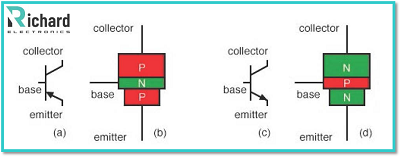
Figure 1 NPN and PNP Transistors
While operating, the proper biasing (polarity) of the junctions is the main functional difference between a PNP transistor and an NPN transistor. “Current-controlled” current regulators are the most common application of bipolar transistors. In other words current passed according to a smaller, controlling current can be restricted by a transistor, depending on the type of transistor it is (NPN or PNP) the main controlled current goes from collector to emitter, or from emitter to collector. The arrow always points in the direction of the current flow in the transistors, according to the standards of semiconductor symbology.
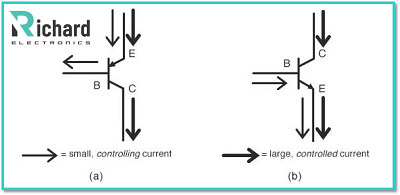
Figure 2 Current flow diagram
Types of Semiconductor Material in bipolar transistors;
As the main flow of current through transistors takes place in two types of semiconductor material: P and N, Bipolar transistors are called bipolar. The main current goes from the emitter to the collector. In other words, the main current is through the transistor. Is compromised by the two types of charge carriers electrons and holes.
The emitter wire mesh together the controlling current and the controlled current in the direction of the transistor’s arrow. In the use of transistors, this is the first and foremost rule. To work as a current regulator all currents must be going in the proper directions for the device. We usually refer to the small controlling current simply as the base current because, through the base wire of the transistor, it is the only current that goes through it. On the other hand, the large controlling current is simply referred to as the collector current because, through the collector wire of the transistor, it is the only current that goes through it. In compliance with Kirchhoff’s Current Law, the sum of the base and collector currents is the emitter current. No amount of the through the base of the transistor shuts it off like an open switch and prevents current flowing through the collector. The proportional amount of current through the collector is allowed by a base current that turns the transistor on like a closed switch.
Key points on bipolar transistors:
· The controlled current must go through two types of semiconductor material: P and N, Bipolar transistors are so named. In different parts of the transistor, the current consists of both electron and hole flow
· P-N-P or an N-P-N semiconductor “sandwich” structure makes the structure of bipolar transistors
· The Emitter, Base, and Collector. These are the three layers of a bipolar transistor.
· By allowing a small current to control a larger current, Transistors function as current regulators. The amount of current moving between the base and emitter determined the amount of current allowed between the collector and emitter.
· The controlling (base) current and the controlled (collector) currents must be going in the proper directions, for a transistor to properly function as a current regulator.
Saturation in (BJT) transistors:
While using BTJs to switch on or off a load for example an LED, the BJT is operated in saturation mode. We will discuss in detail the working of BJTs in saturation mode. And how can ensure saturation by calculating the base resistor?
Circuit Arrangement:
The circuit below illustrates the circuit arrangement for a transistor (Q1) used as a switch to drive a load (150 Ohms Resistor) equipped with a logic signal generated by a logic gate or microcontroller on the left side.
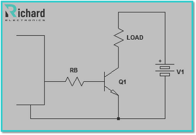
Figure 3 Circuit arrangement for a transistor
No current will flow through the RB when the controlling device's output is low and Transistor is turned off. As a result in the collector circuit, no current flows through the load for example if the LEDs are attached to a load they will not illuminate. And if we are using a coil as load it doesn't energies if it's with a reverse diode across it for back EMF suppression.
On the other, the current will flow through the RB into transistor Q1's base, when the controller device provides high output. It flows into Q1 after flowing through the load, and back to 0 after getting out Q1's emitter. So the LED is lit up or a relay gets activated because the load is energized.
Calculating maximum collector current IC
While calculating the RB value the first step involved is calculating the maximum collector current IC. In the case of using resistive load, by using ohms law we can calculate the IC (max), from load resistance and voltage V1.
On the other hand, if we use an LED with a series of resistors as load, we already know the current because the current is the same in the series type of circuit. Identification of this current and the resistor value helps us to choose an appropriate transistor Q1. The minimum current gain hFE (min) is also an important factor to consider here, the higher the value of hFE, the easier to drive a transistor because of the lower base current value. The current gain will have a lower value for the larger transistor. So choosing an overrated resistor is not an issue (up to 50% higher than IC (max) but not necessarily overrated.
The hFE has an Inverse relationship with the IC, as the value of IC increases the hFE decreases. A typical characteristics graph shows the relationship between these two factors.
Nominal base current IB (nominal)
The second step involves the IB nominal calculation, which can be achieved by dividing the IC with the hFE at that value of the collector current. For example, if we take
IC (max) = 30 mA
hFE (min) = 83
at, IC = 30 mA
then
IB (nominal) = 410 µA
To ensure that the transistor is saturate we multiply the IB (nominal) by a saturation factor that is a number between 2 and 10.
Calculation of RB
We will calculate the base resistor voltage across it. The out can be dragged down somewhat when we are drawing several milliamps from the driving device, this happens often in power devices. To show how much the output will drop while supplying the current can be identified by the datasheet. So the left end of RB illustrates the voltage, and approximately 0.8 V at the right end of the RB. For transistors under bias, this is the approximate base-emitter voltage. For example, consider a device with a +5V voltage supply, and under 1.1 mA its output will drop from 5V to 4.8V. So the value of the resistor across it will be 4.0V.
By using Ohms’ law
R = V/I
V = 4.0
So
R = 4.0/0.0011 = 3636 Ω
To ensure that we get less than that amount of current, we should use a 3k3 or 3k6 resistance value that equals or lower the calculated value.
Saturation factor:
To ensure that the transistor saturates properly a factor between 2 to 10 is needed as mentioned earlier. Generally, the saturation is related to the collector-emitter voltage VCE, but can also be defined in other ways. The diagram below illustrates the LT spice simulation of a transistor driving 160 Ω with a power supply of 5V. When the transistor is turned on it corresponds to about 30 mA. Collector current.
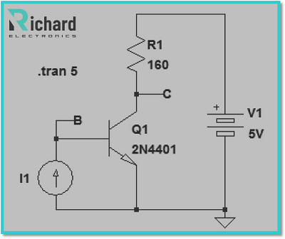
Figure 4 Circuit arrangement for saturation factor
Over a second period of time, the base current is ramped steadily from zero to 5 mA. The straight green line below represents the base current. The red curve represents the collector-emitter voltage over that range. As the emitter is connected to 0V VC and VCE are the same.
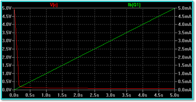
Figure 5 Graph between base current and collector-emitter voltage
Where IC is proportional to IB, the transistor operates in its linear region as shown in the graph.
Saturation region:
The maximum possible current is 31.25 mA with a 5V supply and 160 ohms resistor. As the collector current is limiting the current the transistor cannot increase the collector current. In other words, the collector-emitter voltage is running out in the transistor. Here the power supplied to it is 5V. The resistor would have to drive its collector negative to get more collector current through that fixed load.
This is how saturation looks like and can be defined as “this situation in which the IC is no longer proportional to IB in other words doesn't increase with increase in the IB, When VCE is dropped down a specific voltage, when in collector base junction a certain amount of current is flowing.
While switching On and Off a load, in the On state we want to saturate the device, because we want to maximize the voltage across the load and minimize VCE. This is known as the saturated switch.
The saturation region close-up:
The graph below illustrates the close-up view of IB vs VCE, showing the saturation region only.
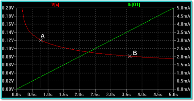
Figure 6 Graph between IB vs VCE
In the above figure, we can see that at ground 120 mV the VCE curve starts, and the point corresponding to IB is marked A which is roughly IB = 750 µA. Increasing the base current ten times that nominal current IB (nominal), at point "B" this is 3.6, from 120 mV to 80 mV the value of VCE drops.
Wastes of base current for no significant drop in VCE. Occurs when we Increasing IB beyond that point enters the area of rapidly diminishing returns. Between 2 IB (nominal) and 10 IB (nominal) the optimum reasonable base current probably lies. How much base current you want to waste determines, where you operate the transistor. Other factors if they are quite variable you may need to take into account are:
· Temperature (at low temperatures if the circuit needs to operate we may need to be more conservative as well for example using a transistor with a higher IB)
· Aging (if the component is stressed hFE deteriorates gradually with age). Other factors may include tolerance in RB individual component variations, peak vs average current (very vital factor), the load, and the supply voltage.
Functions of transistors:
· Here we will focus on the practical functions and applications of bipolar transistors instead of exploring the quantum world of semiconductor theories. Here we will explore the general use of transistors as a component. BJTs are crucial in a wide variety of electrical contexts because of their adaptability from amplification to signal processing their impact may be felt in many areas of technology.
· The BJTS plays a vital role in applications related to amplifying signals. Whether in audio or radio frequency systems, amplifier circuits leverage the current applications capabilities of BTJ to enhance the weak signals.
· As electronic switches, the BTJ shines in digital electronics. In the ability of the transistor to act as a switch the control of current flow between the collector and the emitter plays a vital role. The on state of the transistor and the off state are the two main states of operation for a BJT switch.
· In oscillators, we use transistors because of their ability to generate periodic waveforms. Essential waveforms for applications such as signal generators and radio frequency oscillators are generated by these circuits, playing the role of backbone in communication systems.
· Ensuring a stable output voltage, BJTs play a pivotal role in voltage regulation circuits that are very essential for electronic devices.
· In audio electronics, BJTs are the most useful component in amplifier circuits. They are indispensable for applications where faithful reproduction of sound signals is paramount because of their ability to amplify small inputs.


