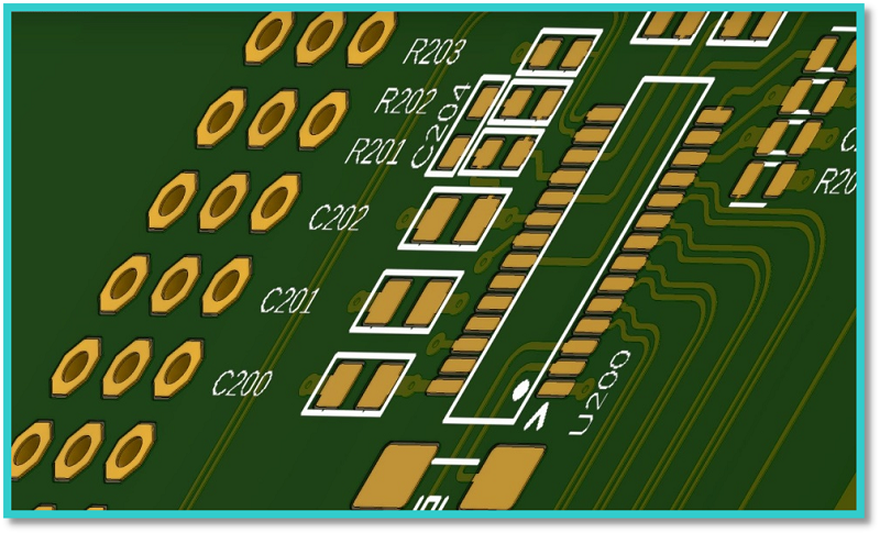
Any professional have experience in designing PCBs has faced the challenge of deciding appropriate trace at some point. The default traces given in the software to design PCBs only work up to a certain extent and are used by inexperienced PCB designers. These default widths can be easily noticed by those who know electronics that these narrow lines are not suitable for some tracks such as for ground connections and power supply.
What is Trace?
A thin line of conducting copper is known as a PCB trace placed on an isolated base material or non-conductive material used to carry power and signal throughout the circuit. This trace of conductive material has a specific width that is known as trace width with a specific thickness and height. Usually, the thickness and height of the copper layer are fixed as per the manufacturing company specifications and decided as per the application. In the United States, the PCB trace width is measured in the ounces per square foot. These traces are also measured in mils and thousands of an inch.
Types of traces:
I. Signal Traces:
Through the signal traces the data is conveyed. Having different trace widths in analog or digital signals does make much difference in simple PCB designs, but these traces play a vital role in high-speed digital designs and RF/Analog. Since trace width and impedance have an inverse relationship trace impedance is an essential consideration.
II. Power Traces:
As the name suggests, the power traces are responsible for carrying power to each component in the circuit, so these traces require more attention.
Factors involved in Trace width:
We need to understand the trace’s difference in a circuit to find the answer to why different trace widths matter. Usually, in a PCB, two types of traces are involved: power traces and signal traces.
I. Current Carrying Capacity:
The most obvious reason for traces is current carrying capacity due to the relationship between the width of the conductor and current carrying capacity. The amount of current a trace can carry is determined by the cross-sectional area of a trace and allowable temperature rise. The copper thickness and trace width are directly proportional to the cross-sectional area of the trace. The temperature also rises when we increase the current passing through the trace.
II. Trace Impedance:
To minimize the crosstalk, coupling and reflection-specific spacing and the impedance may be required for high-speed circuits. The RF analog traces and high-speed traces must be calculated as they are sensitive data lines. The PCB traces don't act like simple connections in the case of high-speed traces. Internal resistance and series inductance are present in every copper trace, which for a simple low-speed design can be overlooked. On the other hand, in high-speed designs, the board's performance is affected by the increase in the trace inductance and copper surface roughness.
III. Signal Reflection:
In high-performance electronics circuits designing signal reflection is an essential issue. Some portion of the transmitted signal reflects toward the source the phenomenon is known as signal reflection, it causes distortion and oscillation so the signal reflection is undesirable. The route of traces and shape affected the signal reflection in PCBs. Whenever a trace changes direction, shape, or interface to a component the trace discontinuities come into play.
Trace width considerations for High Power PCB:
While designing the high-power PCBs we keep the traces short as we know every conductor offers resistivity up to a certain value. Therefore as the trace gets longer and narrow the trace resistance increases. Due to the Joule heat when current passes through the trace higher power losses occur. The longevity of the board is reduced because the wasted power converts to heat. That’s why to prevent blistering, delamination, or fire it is very necessary to keep traces carrying higher currents as short as possible.
Trace width considerations for High-Speed PCB:
Two differential traces should match as closely as possible in length. The rise time requirement and the link’s data rate affect the tolerance to match a signal and its complement. Achieving the desired specification can be done by optimizing the trace width and spacing.

Trace related Specifications:
As a general rule, the bare PCB fabrication costs began to be driven up by the following trace-related specifications. Due to the tighter PCB tolerances and higher-end equipment needed the cost becomes considerably higher to both manufacture and inspect the PCB. Following are the general specifications involved in PCB fabrication.
· The trace width should be narrower than 5 mils.
· The trace width should be closer than 5 mils.
· The diameter for via holes should be smaller than 8 mils.
· 1.4 mils or in other words, one ounce should be the trace thickness or thinner than it.
· The controlled lengths or trace impedance and differential pairs.
The high-pitch BGAs or high signal count parallel buses which are high-density designs incorporating PCB footprints require trace widths as thin as 2.5 mils. In the case of special types of vias 6 mils or less such as for laser drilled micro vias. On the other hand entire layer and at thicker ounce pours than standard is required for some high-power designs. Very thin boards containing several layers and a limited copper pour thickness of half an ounce or 0.7 mils are required for space-constrained applications hence very thin types of boards are required.
In some other cases for different applications traces are required with control impedance and specific width and spacing from each other to minimize reflections and inductive coupling in a design that requires high-speed communication from one peripheral to another. In bus to match with the other associated signals the design might need to be a certain length. Safety is a very important phenomenon while dealing with high voltage applications, to fulfill the requirements of certain safety features such as minimized distance between two exposed differential signals to prevent arcing. So we can conclude that trace definition matters whatever the features or characteristics.


