
Switching Regulator Design Calculator: A Comprehensive Guide
Have you ever felt it tricky to design efficient voltage regulators? A switching regulator design calculator can then help you out. Designing these regulators is essential to convert voltages effectively, but it can get complex and error-prone.
This article will show the use of an online calculator step-by-step. Follow our instructions and tips, and you can confidently deal with your power supply projects, making them reliable and efficient.
So, let's get started.
Understanding Switching Regulators
In essence, switching regulators are electronic devices used to efficiently convert voltage, incorporating elements like inductors and capacitors for energy storage in high-frequency switching.
Unlike linear regulators, which dissipate any excess power as heat, switching regulators switch on and off very quickly, minimizing power loss and optimizing efficiency.
Types of Switching Regulators
1. Buck Converter: Step down an input voltage to a lower output.
2. Boost Converter: Steps up the input voltage to a higher output voltage.
3. Buck-Boost Converter: It may step the input voltage up or down.
4. Flyback Converter: Mostly used in Isolated power supply applications.
Key Components and Operation
Switching regulators work by using a few critical components:
· Inductors: Store energy when the switch is on and release it when the switch is off, smoothing the current.
· Capacitors: Filter the output voltage to improve ripple and noise.
· Switches (Transistors): This simply describes the switching on and off states, which will control energy transfer in a device implementation.
· Control circuits: The switching frequency and duty cycle can be varied through the control to maintain the magnitude of the output voltage.
Introduction to Switching Regulator Design Calculators
Design calculators for switching regulators are a key. They are tools that support engineers in designing and optimizing high-efficiency switching regulator circuits.
Calculators have varied input and provide recommendations for component values, the design of the circuit configuration, and estimates of the performance of the circuit.
Types of Design Calculators
· Software-based Tools: This could range from stand-alone applications to applications fully involved in development environments supporting design and simulation.
· Online Tools: Web-oriented calculators, which report back fast support reactions and pretty rough suggestions of designs.
Step-by-Step Guide to Use Online Switching Regulator Design Calculator
The switching regulator design becomes much easier by having an online switching regulator design calculator that gives exact values of the components and other performance metrics subject to inputs provided by the user.
Here's how you can use switching regulator design calculator tools:
Step #1: Initial Considerations
Please have the following parameters for your switching regulator requirements before you start using the calculator to enter the data.
The basic parameters are:
· Maximum Input Voltage (Vin(max))
· Nominal Input Voltage (Vin(nominal))
· Minimum Input Voltage (Vin(min))
· Output Voltage (Vout)
· Diode Forward Voltage (Vd)
· Maximum Output Current (Imax)
· Minimum Output Current (Imin)
· Maximum Output Voltage Ripple
· Desired Switching Frequency (Fs)
Step #2: Entering Parameters into the Calculator
Now you will have to give all the input data like:
1. Maximum Input Voltage (Vin(max)): Enter the highest voltage the regulator will receive. For instance, if the maximum input voltage from a power source is 15V, input 15V.
2. Nominal Input Voltage (Vin(nominal)): Enter the typical operating voltage. For example, if the nominal voltage is 12V, input 12V.
3. Minimum Input Voltage (Vin(min)): Specify the lowest voltage the regulator might receive. If the minimum voltage is 10V, input 10V.
4. Output Voltage (Vout): Enter the desired stable output voltage, such as 5V for many digital circuits.
5. Diode Forward Voltage (Vd): Input the forward voltage of the diode used in the circuit. For instance, if the forward voltage is 0.7V, input 0.7V.
6. Maximum Output Current (Imax): Specify the highest current the regulator must supply. For example, if the maximum current is 2A, input 2A.
7. Minimum Output Current (Imin): Enter the lowest current the regulator needs to supply. If it's 0.1A, input 0.1A.
8. Maximum Output Voltage Ripple: Input the acceptable ripple voltage at the output. For instance, if the maximum ripple is 50mV, input 50mV.
9. Current Sense Resistor: If unsure, use a default value such as 0.01 ohms. Enter 0.01 ohms.
10. Top Feedback Resistor (Rf1): Typically, 10K ohms is used if unsure. Enter 10K ohms.
11. Desired Switching Frequency (Fs): Choose the switching frequency for the regulator. For example, if the desired frequency is 100 KHz, input 100 KHz.
12. MOSFET On Time and Off Time: Enter the expected on and off times for the MOSFET in nanoseconds. For example, if the on time is 200ns and the off time is 800ns, input these values.
13. MOSFET Gate Charge: Specify the gate charge in nanocoulombs. For instance, if it's 25nC, input 25nC.
Step #3: Analyzing the Results
After entering the parameters, you will have to hit the Compute button and the calculator will provide several critical outputs:
· Duty Cycle (%): The percentage of time the MOSFET is on during each cycle.
· Ton(min) and Ton(max): The minimum and maximum switch-on times in nanoseconds.
· Maximum Diode Power (W): The maximum power dissipated by the diode.
· Maximum LM25085 Power (W): Power dissipated by the regulator IC.
· Maximum Current Sense Resistor Power (W): Power dissipated by the current sense resistor.
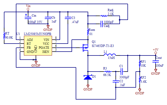
1) Component Selection
The calculator will suggest the following component values:
· Inductor (L): Specified in microhenries (uH), this value is critical for energy storage.
· Current Limit (Icl): The peak inductor current, specified in amps.
· Output Capacitor (Cout): Specified in microfarads (uF), crucial for smoothing the output voltage.
· Input Capacitor (Cin): Also specified in microfarads (uF), important for filtering the input voltage.
· Rf2: The bottom feedback resistor value in kilo-ohms (Kohms).
· RT: Timing resistor value in kilo-ohms (Kohms).
· Radj: Adjustment resistor value in ohms.
· Cadj: Adjustment capacitor value in picofarads (pf).
· R3 * C1 Product: This product helps in stability and compensation, where R3 is in kilo-ohms (Kohms) and C1 is in picofarads (pf).
· R3 and C2: Individual values for R3 (in K-ohms) and C2 (in microfarads) for compensation.
2) Adjusting Parameters for Optimization
Optimization involves refining the design based on the calculator's initial recommendations:
1. Fine-tuning the Inductor Value: Adjust the inductor to balance between transient response and ripple current.
2. Selecting Capacitors: Ensure the output capacitor (Cout) minimizes ripple within the specified limits. Similarly, choose an input capacitor (Cin) that adequately filters the input voltage.
3. Optimizing Resistors and Capacitors: Adjust feedback resistors (Rf1 and Rf2) and timing components (RT, Radj, Cadj) to fine-tune the regulator's response and stability.
4. Duty Cycle Adjustments: Ensure the duty cycle remains within acceptable limits to avoid excessive stress on the MOSFET and other components.
By following these steps, you can effectively use the switching regulator design calculator to achieve a well-optimized and reliable power supply design.
Benefits of Using an Online Design Calculator
Adopting a web-based design calculator for switch regulators opens benefits that allow more tremendous success through attaining higher efficiency, precision, and general success in designing a product.
Some of the most important benefits are:
1. Enhanced Accuracy and Precision
The design calculators use sophisticated algorithms and extensive databases to offer precise values of components and design recommendations.
This feature reduces the margin of errors found when creating manual calculations and consequently can influence potential changes in the design about the specifications required.
2. Time Efficiency
The design of switching regulators is iterative by its inherent nature, which always includes more than one figure.
An online calculator can reduce this to around several seconds because component and performance figures are displayed instantly with changes in user input, so rapid computing is enabled, and the designer has more time to test their designs and provide the most significant amount of optimization effort.
3. Simplified Component Selection
Online calculators help engineers specify proper components for inductors, capacitors, and ranged items through MOSFETs. The calculator recommends specific values and types for a correct operation with a set of input parameters.
Thereby, design engineers do not have to go through the often intricate procedure of correctly sizing and choosing a component that will be compatible and optimum in performance.
4. Design Optimization
These tools typically provide options to tune the parameters so an engineer can iteratively assign values to parameters such as switching frequency, output voltage ripple, and duty cycle toward achieving an optimum design concerning efficiency, size, and thermal requirements.
Owing to this flexibility, more refined and practical designs can be realized.
05. Reduced Risk of Human Error
Manual processes are inherently prone to human error, and it may culminate in a disastrous design flaw. These online calculators help in mechanizing calculations that then decrease the chances of a mistake and, in turn, increase the dependability of a design.
This will ensure a more accurate prediction that the design will work for the specified requirements.
06. Up-to-Date Component Information
Online calculators are regularly updated with the latest information on components and design methodologies. This periodical updating of information ensures the recommendations are current with new technologies and best practices.
Common Mistakes to Avoid Using Online Switching Regulator Design Calculator
Though design calculators for switching regulators conveniently save from any annoyance and bring a variety of benefits with their use, it is obligatory to use them correctly in order not to fall into standard pitfalls.
Here are some typical mistakes:
1. Incorrect Parameter Inputs
Equivocating on the part of one critical parameter in the sense of putting it wrong or disseminating inaccurate values, for instance, the input voltage, output voltage, load current, or switching frequency, makes the results incorrect.
Ensure all inputs are as accurate as possible. Ensure the entered values are conditions as in the real world under which the regulator will function. It is better to have the measurements of absolute voltages and supplied currents instead of theoretical values used in calculations.
2. Overlooking Diode Forward Voltage
The result will become an error for the estimation of output voltages and efficiencies because the forward voltage of the diode is one missing document here.
If in doubt, quote the diode forward voltage from the datasheet for the diode in question. Otherwise, a typical value from the calculator or manufacturer guidance would be acceptable.
3. Ignoring Temperature Effects
Not accounting for temperature variations that can affect component performance and regulator stability.
Be mindful of application temperature ranges. Use parts rated for the maximum expected temperature, and let the calculator settings account for this environment. Look for thermal performance information in the calculator output.
4. Inadequate Ripple and Noise Considerations
Failure to specify the maximum allowable output voltage ripple correctly can lead to designs that fail to meet the requirements of noise-sensitive applications.
Reducing the output capacitor to the minimum allowed value will ensure minimum output voltage ripple.
Frequently, the reduction of necessary output filtering capacitors is the suggestion for cost or size savings, leading to increased output ripple in linear regulators.
Additional Practical Tips and Best Practices for Your Help!
Here are some tips to help you achieve the best results:
· Double-Check Input Values
Just double-check your input values concerning quantities you are plugging into the calculator; minor errors will produce the wrong suggestions for components and will compromise the performance needed to meet your goals.
Make sure you measure the actual operating conditions of your circuit with an accurate measurement tool rather than relying straight on the circuit's theoretical values/assumptions.
· Understand the Impact of Each Parameter
Take some time to understand how exactly each parameter modifies an overall design. For instance, how precisely does a change in switching frequency influence efficiency and component size correction?
Play with the various values in the calculator. You can get to see how the advisable topologies and performance numbers change with this and just learn more about the trade-offs entailed in switching regulator design.
· Component Quality and Specifications
Quality high-grade components should be used, meeting or exceeding the suggested specifications of the calculator. Pay particular attention to things like voltage ratings, current ratings, and thermal performance.
Refer to datasheets and manufacturer's guidelines to ensure that environment conditions are suitable for the application and operating conditions of the components selected.
Final Thoughts
In conclusion, switching regulator calculations are typically complex, online design calculators can remarkably reduce the design process time and increase its efficiency and accuracy.
By understanding the basics of switching regulators and using these calculators correctly, engineers can optimize their designs to meet specific requirements.
ALSO SEE:All Online Conversion Calculators by Richard


