
Historical Background
Hans Camenzind designed the timer IC in 1971 in a contract with Signetics. Signetics hired him in 1968 to develop an IC phase-locked loop (PLL). An oscillator for PLLs was designed so that the frequency may not depend on the temperature or power supply voltage. Eventually, Signetics dismissed half of their employees because of the economic decline in 1970, and improvement in the PLL was stopped. The development of a universal circuit was proposed by Camenzind, depending on the oscillator for PLLs, and he said that he improved it independently. Taking the equipment on a loan basis from Signetics despite getting his half salary. The idea of Camenzind was rejected thereafter remaining engineers declared the equipment might be built from the sold parts of the company and the manager of the marketing department agreed on the idea.
In 1971 summers, the first design for 555 was evaluated. As the discussed design was tested and observed to be errorless, Camenzind discovered the plan of using a resistance-direct despite a constant current source, discovering that the working is adequate. The changed design decreased from the external 9 pins to 8, so the IC might easily fit in a package of 8 pins despite a package of 14 pins. The revised status moved the second review of the design, in October 1971 the prototypes were completed as the SE555t (metal TO-5) and NE555V (DIP Plastic). An engineer from another company already discovered the 9-pin version, he had attended the first version and retired from Signetics; the firm released its innovation right after the 555 was reviewed. In 1972, 12 companies manufactured the 555 timer and the product became the bestselling among all.
Besides timers, there are many applications of 555. In 1997, Camenzind realized that 90% of its applications were in fields that he never observed. For several months, he was overwhelmed by engineers who had innovative ideas for using the device.
Introduction
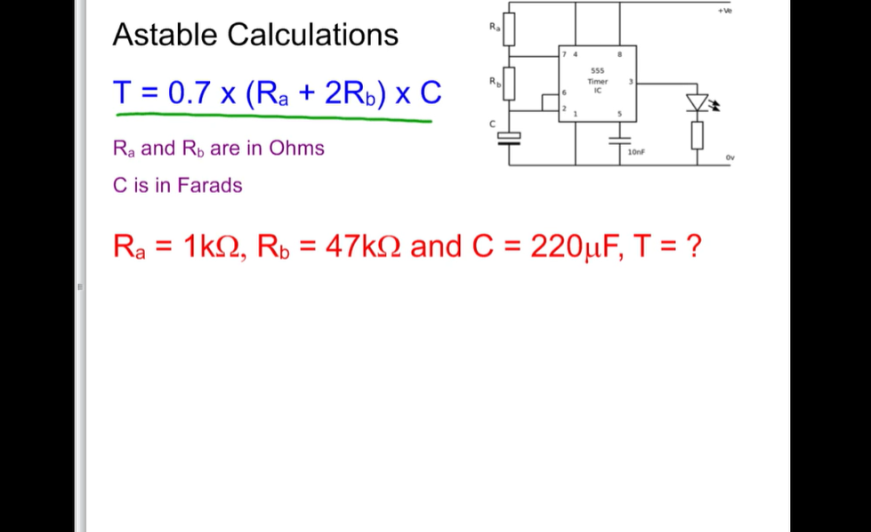
The name of IC 555 Timer was derived from the three resistors 5KΩ5KΩ also used in voltage divider network. This type of IC is beneficial for producing oscillators and time delays.
Pin Diagram and Functional Diagram
Let's discuss the 555 Timer IC pin diagram and the functional diagram.
Pin Diagram
The IC 555 Timer is an 8-pin Dual Inline mini package (DIP). The pin diagram of a 555 IC Timer is presented below

Figure 1 Pin Diagram for 555 Timer IC
The importance of each pin in the Timer is self-explanatory. An +5V to +18V DC supply can operate this 555 IC Timer. It is usually used for producing non-sinusoidal waveforms for example ramp, pulse, square, etc.
Functional Diagram
The figure below represents the internal details of a 555 Timer IC and is known as a Functional diagram.
Note that the operating diagram of 555 Timer IC consists of a Voltage divider network, one SR flip–flop, two comparators, two transistors, and an inverter. The purpose of each component is discussed in detail

Figure 2 Functional Diagram of 555 IC Timer
Voltage Divider Network
· This component contains three resistors 5KΩ5KΩ that are in series attached with the supply voltage VccVcc and ground.
· The voltage divider network provides a voltage of Vcc3Vcc3 between the ground and a point if it has only one resistor 5KΩ5KΩ. Same as if it supplies a voltage of 2Vcc32Vcc3 between ground and a point if it has only two resistors 5KΩ5KΩ.
Comparator
· The operating diagram of a 555 IC timer contains two comparators: An Upper comparator (UC) and a Lower Comparator (LC)
· Remember that the comparator differentiates the two inputs applied to it and generates an output.
· In an OP Amp, if the voltage level at the non-inverting terminal is higher than the voltage at the inverting terminal, then the product of the comparator will be +Vsat+Vsat. In digital presentation, it can be taken as Logic Low (0)
SR Flip-Flop
· The SR flip-flop deals with a positive clock transition or a negative clock transition. It contains two inputs, S and R, and the two outputs: Q(t) and Q(t)’. The two outputs Q(t) and Q(t)’ are complement to each other.
· The below-mentioned table presents the state table of an SR flip-flop

· Above, Q(t) and Q(t +1) show the state and its next state accordingly. Thus SR flip-flop is beneficial for one of three functions for example Hold, reset, and Set, and are dependent on the input when the signal is applied (positive or negative transition of clock)
· The outputs from an Upper comparator (UC) and a Lower Comparator (LC) are taken as inputs of SR flip-flop as presented in the functional diagram of 555 Timer IC.
Transistors and Inverter
· The operating diagram of a 555 timer IC contains, one npn transistor Q1Q1 and a pnp transistor Q2Q2. The npn transistor Q1Q1 will be operating as On if its voltage at base to emitter is positive and higher than cut in voltage. If not, it will be operating as Off.
· For buffer, the pnp transistor Q2Q2 is used in such a way to separate the input reset from the npn transistor Q1Q1 and SR flip-flop.
· In the 555 Timer IC, the inverter used not only plays the inverting action role but also amplifies the power level.
The 555 Timer IC is also beneficial for uni-stable working for the generation of a pulse at the output. Moreover, at output, it can also be used in a stable operation in a way to generate a square wave.
555 IC Applications
This type of IC connects external capacitors, resistors, and several components that can be used as:
· Single stable trigger, beneficial in timing delay shaping and timing switches.
· As we know the Multivibrator, produces a signal-generating circuit.
· Schmitt trigger is also beneficial as it is used in the shaping circuit, pulse amplitude discrimination TTL system interface, etc.
I. A monostable trigger is useful for timing delay shaping and some switches of timing.
Let's suppose that the resultant output at a low level is stable, however, under the impact of external conditions, the output becomes the transient steady state which means that the output for the time being changes to the higher level but somehow becomes at a low level. An example, a delayed turn-off light is designed with a monostable feature. Suppose after the turn-off, suddenly it will not be powered off but a time of delay that can be itself operating.
The combination of 555 timers and the delay set produced by the RC series combination can be converted into a monostable flip-flop. At the input terminal, if IN2 is used the trigger signal and to simulate the control signal K1 is used. Neglecting the fact that IN2 is high, but it gets low when K1 is pressed. By connecting the capacitor C1 and resistor R1 in series, between the GND and Vcc, the point of the resistor-capacitor connection is attached to the transistor of the collector inside the 555 and IN1. The terminal at output uses 2 different LEDs to show the circuit output level.
Suppose that the circuit board is securely turned on, and the key K1 is not pressed (IN2 = Vcc). At this point, the output of this timer is not easy to calculate so it might be discussed solely. Let's suppose the timer output is very low. If at the Capacitor C1, the charge is stored, it would be sharply discharged from the transistor that is turned on. So IN1 = 0<VH, IN2=Vcc>VL, keeping in view the function table parameter, the 555 output will stay the same at the point. That state is called a stable state.
Suppose the timer output is very high, at this state the transistor acts as off and Vcc charges the resistor from the capacitor. Moreover, if the voltage of the capacitor is IN1>VH, it is called IN2>VL, sp the timer output is at a low state, the transistor is turned on and works back to its previous state. So the maximum level is the transient steady state and the process duration from the capacitor to charge is the time until the VH is less than the voltage.
At the point when no trigger signal is there, the 555 timer state output will be stable. In case the down edge of the trigger pulse becomes IN2, so IN2<VL, also at the same moment, due to IN1<VH, the timer gives a high output, and the transistor is cut off, it becomes a steady state transient. After some time it behaves in a steady state.
At the output signal, the high-level period is the transient steady state and the moment it gets to charge the capacitor to VH. This period can be determined keeping in view the relationship between the charge and discharge of RC which is equal to a time constant of 1.1 times.
II. Multivibrator forms a signal-generating circuit.
It is a kind of free-running oscillator. When the power is on, without an external trigger signal the rectangular pulse automatically can be produced. As the rectangular wave gets rich harmonic components in high order, it is necessary to say multivibrator, the rectangular wave oscillator also in some data called as nonstable mode. Earlier, a rectangular wave-producing circuit was executed with a Schmitt trigger. Since the timer 555 can also be beneficial for the Schmitt trigger, on this basis, it is not complicated to use as a multivibrator. As for usage, it can also produce a dual-color light that flashes one by one.
Initially, attach the both IN1 and IN2 altogether and produce a Schmitt trigger.
After that using the voltage capacitor as the input signal, and tracing a way to set a capacitor voltage between the two different thresholds of the Schmitt trigger. By connecting the 555 timer output to the capacitor, when the output is maximum level charge the capacitor, and when the output is low discharge the capacitor. Moreover, in reality, to lessen the load of the 555 timer, Vcc is utilized for capacitor charging and is discharged by a discharge transistor. When a Vcc is connected to the triode with the help of a resistor, the level of the collector triode (7 number pin of the 555 timer) is equal to the output.

Figure 3 555 IC Timer as Multivibrator
III. Schmitt Trigger, is beneficial for the interface of TTl system, pulse amplitude discrimination, shaping circuit, etc. These have several different threshold voltages for signals at input with dual changing directions, which are decreasing negatively and increasing positively.

Figure 4 555 IC Timer as Schmitt Trigger
If the 2 terminals of input are connected as a new input terminal in a way to get a Schmitt trigger. Most of the time, to improve the stability of the circuit a capacitor is attached to Cont. Instead of connecting it to the reference voltage externally, VH = 2/3Vcc, VL =1/3 Vcc. So keep the input signal to Vi. The method is slowly increasing from 0:
1. Vi < VL < VH, Vc1= 0, Vc2 = 1, out=1.
2. VL < Vi <VH, Vc1= 0, Vc2= 0, out is same as 1.
3. VL <VH <Vi, Vc1= 1, Vc2= 1, out=0.
Later, Vi keeps on changing, but the output will remain the same, so calculate the process of VH from being smaller than Vi.
4. VL < Vi < VH, Vc1= 0, Vc2= 0, out remains same that is 0.
5. Vi < VL < VH, Vc1= 0, Vc2= 1, out=1.
Conclusions
The 555 IC timer is a stable, powerful, and frequently used integrated circuit in the field of electronics and is also used in many electronics circuits. The IC 555 produces the square wave and the duty cycle ranges from 50 % to 100%. The delay in the period is given by an oscillator. It is a monostable multi-vibrator that uses a 555 timer, the output remains in a low state while the input is triggered. This type of system is beneficial in the push-to-work system. Moreover, if the input is triggered then the output will move to the maximum state and get to its genuine position back.
ALSO SEE:All Online Conversion Calculators by Richard